
- 非IC关键词
企业档案
- 相关证件:

- 会员类型:普通会员
- 萧先生

- 电话:0755-82725721/82799011
- 手机:13823700718
- 地址:公司地址:深圳市福田区中航路新亚洲国利大厦10楼1010室
- 传真:0755-82546403
- E-mail:XEP0718@163.COM
产品分类
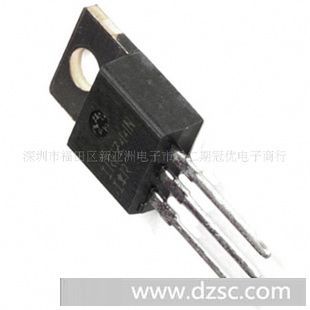

供应原装功率场效应管IRFZ44N
IR/国际整流器
IRFZ44N
*缘栅(MOSFET)
N沟道
增强型
L/功率放大
55(V)
49000(mA)
产品信息
Philips Semiconductors Product specification
N-channel enhancement mode IRFZ44N
TrenchMOSTM transistor
GENERAL D*CRIPTION QUICK REFERENCE DATA
N-channel enhancement mode SY*OL PARAMETER MAX. UNIT
standard level field-effect power
transistor in a plastic envelope using VDS Drain-source voltage 55 V
’trench’ technology. The device ID Drain current (DC) 49 A
features very low on-state resistance Ptot Total power dissipation 110 W
and has integral zener diodes giving Tj Junction temperature 175 °C
*D protection up to 2kV. It is RDS(ON) Drain-source on-state 22 mW
intended for use in switched mode resistance VGS = 10 V
power supplies and general purpose
switching applications.
PINNING - TO220AB PIN CONFIGURATION SY*OL
PIN D*CRIPTION
1 gate
2 drain
3 source
tab drain
LIMITING VALU*
Limiting values in accordance with the Absolute Maximum System (IEC 134)
SY*OL PARAMETER CONDITIONS MIN. MAX. UNIT
VDS Drain-source voltage - - 55 V
VDGR Drain-gate voltage RGS = 20 kW - 55 V
&plu*n;VGS Gate-source voltage - - 20 V
ID Drain current (DC) Tmb = 25 °C - 49 A
ID Drain current (DC) Tmb = 100 °C - 35 A
IDM Drain current (pulse peak value) Tmb = 25 °C - 160 A
Ptot Total power dissipation Tmb = 25 °C - 110 W
Tstg, Tj Storage & operating temperature - °C
*D LIMITING VALUE
SY*OL PARAMETER CONDITIONS MIN. MAX. UNIT
VC Electrostatic discharge capacitor Human body model - 2 kV
voltage, all pins (100 pF, 1.5 kW)
THERMAL R*ISTANC*
SY*OL PARAMETER CONDITIONS TYP. MAX. UNIT
Rth j-mb Thermal resistance junction to - - 1.4 K/W
mounting base
Rth j-a Thermal resistance junction to in free air 60 - K/W
ambient
d
g
1 2 3 s
tab
February 1999 1 Rev 1.000
Philips Semiconductors Product specification
N-channel enhancement mode IRFZ44N
TrenchMOSTM transistor
STATIC CHARA*ERISTICS
Tj= 25°C unless otherwise specified
SY*OL PARAMETER CONDITIONS MIN. TYP. MAX. UNIT
V(BR)DSS Drain-source breakdown VGS = 0 V; ID = 0.25 mA; 55 - - V
voltage Tj = -55°C 50 - - V
VGS(TO) Gate threshold voltage VDS = VGS; ID = 1 mA 2.0 3.0 4.0 V
Tj = 175°C 1.0 - - V
Tj = -55°C - - 4.4
IDSS Zero gate voltage drain current VDS = 55 V; VGS = 0 V; - 0.05 10 mA
Tj = 175°C - - 500 mA
IGSS Gate source leakage current VGS = &plu*n;10 V; VDS = 0 V - 0.04 1 mA
Tj = 175°C - - 20 mA
&plu*n;V(BR)GSS Gate source breakdown voltage IG = &plu*n;1 mA; 16 - - V
RDS(ON) Drain-source on-state VGS = 10 V; ID = 25 A - 15 22 mW
resistance Tj = 175°C - - 42 mW
DYNAMIC CHARA*ERISTICS
Tmb = 25°C unless otherwise specified
SY*OL PARAMETER CONDITIONS MIN. TYP. MAX. UNIT
gfs Forward transconductance VDS = 25 V; ID = 25 A 6 - - S
Ciss Input capacitance VGS = 0 V; VDS = 25 V; f = 1 MHz pF
Coss Output capacitance pF
Crss Feedback capacitance pF
Qg Total gate charge VDD = 44 V; ID = 50 A; VGS = 10 V - - 62 nC
Qgs Gate-cource charge - - 15 nC
Qgd Gate-drain (miller) charge - - 26 nC
td on Turn-on delay time VDD = 30 V; ID = 25 A; - 18 26 ns
tr Turn-on rise time VGS = 10 V; RG = 10 W - 50 75 ns
td off Turn-off delay time Resistive load - 40 50 ns
tf Turn-off fall time - 30 40 ns
Ld Internal drain inductance Measured from contact screw on - 3.5 - nH
tab to centre of die
Ld Internal drain inductance Measured from drain lead 6 mm - 4.5 - nH
from package to centre of die
Ls Internal source inductance Measured from source lead 6 mm - 7.5 - nH
from package to source bond pad
REVERSE DIODE LIMITING VALU* AND CHARA*ERISTICS
Tj = 25°C unless otherwise specified
SY*OL PARAMETER CONDITIONS MIN. TYP. MAX. UNIT
IDR Continuous reverse drain - - 49 A
current
IDRM Pulsed reverse drain current - - 160 A
VSD Diode forward voltage IF = 25 A; VGS = 0 V - 0.95 1.2 V
IF = 40 A; VGS = 0 V - 1.0 -
trr Reverse recovery time IF = 40 A; -dIF/dt = 100 A/ms; - 47 - ns
Qrr Reverse recovery charge VGS = -10 V; VR = 30 V - 0.15 - mC
February 1999